
- Manufacturer Part Number : AD8582ARZ
- Manufacturer : AD
- Description : +5 Volt, Parallel Input Complete Dual 12-Bit DAC IC
- Series : AD8582
- Reference Price : USD 13.392
- Our Price : We have a better price, contact us by email
- Product Type : Precision D/A Converters
- Function : Voltage Output D/A Converters
- Current Suggest : Production
- Status : Production
- ROHS Status : ROHS Compliant (Lead Free)
- Package Type : 24-Lead SOIC (Wide)
- Pins : 24
- MFG Package Case : RW-24
- Part Type : OTH
- Standard Packing Type : Tube
- Standard Packing Quantity : 31
- Working Temperature : -40 to 85C
- Other Part Number : AD8582ARZ
- Shipping methods : DHL FEDEX UPS TNT
- Delivery Time : Ship within 1 day.
- Manufacturer Production time : 6-8 weeks (Normally have stocks)
- Weight : 0.001KG
Contact us to check the best price and real time inventory quantity for AD8582ARZ. If you need any more information about AD8582ARZ, you can also send us by email. Our email is [email protected], we will reply you in 12 hours.
- Complete Dual 12-Bit DAC
- No External Components
- Single +5 Volt Operation
- 1 mV/Bit with 4.095 V Full Scale
- True Voltage Output, ±5 mA Drive
- Very Low Power: 5 mW
The AD8582 is a complete, parallel input, dual 12-bit, voltage output DAC designed to operate from a single +5 volt supply. Built using a CBCMOS process, this monolithic DAC offers the user low cost, and ease-of-use in +5 volt only systems.
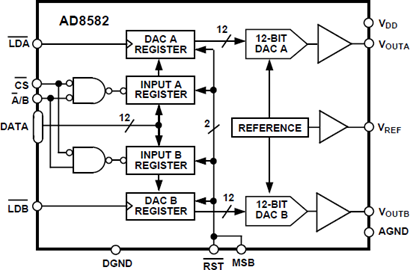
Included on the chip, in addition to the DACs, are a rail-to-rail amplifier, latch and reference. The reference (VREF) is trimmed to 2.5 volts output, and the on-chip amplifier gains up the DAC output to 4.095 volts full scale. The user needs only supply a +5 volt supply.>/p>
The AD8582 is coded natural binary. The op amp output swings from 0 volt to +4.095 volts for a one-millivolt-per-bit resolution, and is capable of driving ±5 mA. Operation down to 4.3 V is possible with output load currents less than 1 mA.
The high speed parallel data interface connects to the fastest processors without wait states. The double-buffered input structure allows the user to load the input registers one at a time, then a single load strobe tied to both LDA + LDB inputs will update both DAC outputs simultaneously. LDA and LDB can also be activated independently to immediately update their respective DAC registers. An address input decodes DAC A or DAC B when the chip select CS input is strobed. An asynchronous reset input sets the output to zero scale. The MSB bit can be used to establish a preset to midscale when the reset input is strobed.
The AD8582 is available in the 24-pin plastic DIP and the surface mount SOIC-24. Each part is fully specified for operation over -40°C to +85°C, and the full +5 V ±5% power supply range.
At least one model within this product family is in production and available for purchase. The product is appropriate for new designs but newer alternatives may exist.


