
- Manufacturer Part Number : AD9119
- Manufacturer : AD
- Description : 11-Bit, 5.7 GSPS, RF Digital-to-Analog Converter
- Series : AD9119
- Reference Price : USD 39.2
- Our Price : We have a better price, contact us by email
- Product Type : High Speed D/A Converters ≥30MSPS
- Function : Standard High Speed D/A Converters
- Current Suggest : Recommended for New Designs
- Status : Production
- RoHS Status: -
- Voltage: -
- Feature: -
- Package Case: -
- Temperature Range: -
- Packing: Reel/Tray/Tube
- Standard Packing Quantity: -
- Country of Origin: -
- Other Part Number : AD9119
- Shipping methods : DHL FEDEX UPS TNT
- Delivery Time : Ship within 1 day.
- Manufacturer Production time : 6-8 weeks (Normally have stocks)
- Weight : 0.001KG
Contact us to check the best price and real time inventory quantity for AD9119. If you need any more information about AD9119, you can also send us by email. Our email is [email protected], we will reply you in 12 hours.
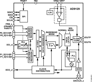
The AD9119/AD9129 are high performance, 11-/14-bit RF digital-to-analog converters (DACs) supporting data rates up to 2.85 GSPS. The DAC core is based on a quad-switch architecture that enables dual-edge clocking operation, effectively increasing the DAC update rate to 5.7 GSPS when configured for Mix-Mode™ or 2× interpolation. The high dynamic range and bandwidth enable multicarrier generation up to 4.2 GHz.
In baseband mode, wide bandwidth capability combines with high dynamic range to support from 1 to 158 contiguous carriers for CATV infrastructure applications. A choice of two optional 2× interpolation filters is available to simplify the postreconstruction filter by effectively increasing the DAC update rate by a factor of 2. In Mix-Mode operation, the AD9119/AD9129 can reconstruct RF carriers in the second and third Nyquist zone while still maintaining exceptional dynamic range up to 4.2 GHz. The high performance NMOS DAC core features a quad-switch architecture that enables industry-leading direct RF synthesis performance with minimal loss in output power. The output current can be programmed over a range of 9.5 mA to 34.4 mA.
The AD9119/AD9129 include several features that may further simplify system integration. A dual-port, source synchronous LVDS interface simplifies the data interface to a host FPGA/ASIC. A differential frame/parity bit is also included to monitor the integrity of the interface. On-chip delay locked loops (DLLs) optimize timing between different clock domains.
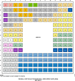
A serial peripheral interface (SPI) configures the AD9119/ AD9129 and monitors the status of readback registers. The AD9119/AD9129 are manufactured on a 0.18 μm CMOS process and operates from +1.8 V and −1.5 V supplies. It is supplied in a 160-ball chip scale package ball grid array.
Product Highlights
- High dynamic range and signal reconstruction bandwidth support RF signal synthesis of up to 4.2 GHz.
- Dual-port interface with double data rate (DDR) LVDS data receivers supports 2850 MSPS maximum conversion rate.
- Manufactured on a CMOS process; a proprietary switching technique enhances dynamic performance.
Applications
- Broadband communications systems
- CMTS/VOD
- Wireless infrastructure: W-CDMA, LTE, point-to-point
- Instrumentation, automatic test equipment (ATE)
- Radar, jammers
This product has been released to the market. The data sheet contains all final specifications and operating conditions. For new designs, ADI recommends utilization of these products.


