
- Manufacturer Part Number : EVAL-AD5696RSDZ
- Manufacturer : AD
- Description : Dual 12-Bit nanoDAC+™ with 2 ppm/°C Reference, I2C Interface IC
- Series : AD5697R
- Reference Price : USD 0
- Our Price : We have a better price, contact us by email
- Product Type : Precision D/A Converters
- Function : Voltage Output D/A Converters
- Current Suggest : Recommended for New Designs
- Status : Production
- ROHS Status : ROHS Compliant (Lead Free)
- Package Type : Evaluation Board for the AD5696R DAC. This board can also be used to evaluate the AD5696 and AD5697R DAC.
- Pins : -
- MFG Package Case : -
- Part Type : EVAL
- Standard Packing Type : -
- Standard Packing Quantity : -
- Working Temperature : -
- Other Part Number : EVAL-AD5696RSDZ
- Shipping methods : DHL FEDEX UPS TNT
- Delivery Time : Ship within 1 day.
- Manufacturer Production time : 6-8 weeks (Normally have stocks)
- Weight : 0.001KG
Contact us to check the best price and real time inventory quantity for EVAL-AD5696RSDZ. If you need any more information about EVAL-AD5696RSDZ, you can also send us by email. Our email is [email protected], we will reply you in 12 hours.
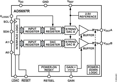
The AD5697R, a member of the nanoDAC+™ family, is a low power,dual, 12-bit buffered voltage output digital-to-analog converter(DAC). The device includes a 2.5 V, 2 ppm/°C internal reference(enabled by default) and a gain select pin giving a full-scale outputof 2.5 V (gain = 1) or 5 V (gain = 2). The AD5697R operates froma single 2.7 V to 5.5 V supply, is guaranteed monotonic by design,and exhibits less than 0.1% FSR gain error and 1.5 mV offseterror performance. The device is available in a 3 mm × 3 mmLFCSP and a TSSOP package.
The AD5697R also incorporates a power-on reset circuit and aRSTSEL pin that ensure that the DAC outputs power up to zeroscale or midscale and remain there until a valid write takesplace. It contains a per channel power-down feature that reducesthe current consumption of the device to 4 µA at 3 V while inpower-down mode.
The AD5697R uses a versatile 2-wire serial interface that operatesat clock rates up to 400 kHz and includes a VLOGIC pin intendedfor 1.8 V/3 V/5 V logic.
Product Highlights
- Precision DC Performance.
TUE: ±0.1% of FSR maximum
Offset error: ±1.5 mV maximum
Gain error: ±0.1% of FSR maximum - Low Drift 2.5 V On-Chip Reference.
2 ppm/°C typical temperature coefficient
5 ppm/°C maximum temperature coefficient - Two Package Options.
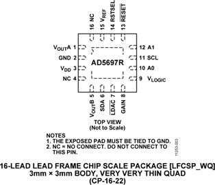
3 mm × 3 mm, 16-lead LFCSP
16-lead TSSOP
Applications
- Base station power amplifiers
- Process controls (programmable logic controller [PLC] I/O cards)
- Industrial automation
- Data acquisition systems
This product has been released to the market. The data sheet contains all final specifications and operating conditions. For new designs, ADI recommends utilization of these products.


