Datasheet for HMC850:

- Manufacturer Part Number : HMC850
- Manufacturer : AD
- Description : 28 Gbps 1:2 Fanout Buffer with Programmable Output Voltage
- Series : HMC850
- Reference Price : USD 0
- Our Price : We have a better price, contact us by email
- Product Type : Logic Devices
- Function : Fanout Buffers
- Current Suggest : Recommended for New Designs
- Status : Production
- RoHS Status: -
- Voltage: -
- Feature: -
- Package Case: -
- Temperature Range: -
- Packing: Reel/Tray/Tube
- Standard Packing Quantity: -
- Country of Origin: -
- Other Part Number : HMC850
- Shipping methods : DHL FEDEX UPS TNT
- Delivery Time : Ship within 1 day.
- Manufacturer Production time : 6-8 weeks (Normally have stocks)
- Weight : 0.001KG
Contact us to check the best price and real time inventory quantity for HMC850. If you need any more information about HMC850, you can also send us by email. Our email is [email protected], we will reply you in 12 hours.
- Inputs Terminated Internally to 50 Ohms
- Differential Inputs are DC Coupled
- Propagation Delay: 75 ps
- Fast Rise and Fall Times: 16 / 15 ps
- Programmable Differential Output Voltage Swing: 600 - 1100 mV
- Power Dissipation: 315 mW
- 16 Lead Ceramic 3x3mm SMT Package: 9mm²
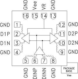
The HMC850LC3 is a 1:2 Fanout Buffer designed to support data transmission rates up to 28 Gbps, and clock frequencies as high as 20 GHz. All differential inputs and outputs are DC coupled and terminated on chip with 50 Ohm resistors to the positive supply, ground. The outputs may be used in either singleended or differential modes, and should be AC or DC coupled into 50 Ohm resistors connected to ground.
The HMC850LC3 also features an output level control pin, VR which allows for loss compensation or for signal level optimization. The HMC850LC3 operates from a single -3.3V DC supply and is available in a ceramic RoHS compliant 3x3 mm SMT package.
Applications
- RF ATE Applications
- Broadband Test & Measurement
- Serial Data Transmission up to 28 Gbps
- Clock Buffering up to 20 GHz
This product has been released to the market. The data sheet contains all final specifications and operating conditions. For new designs, ADI recommends utilization of these products.