
- Manufacturer Part Number : EVAL-24TSSOPEBZ
- Manufacturer : AD
- Description : 8 Channel CMOS Logic to High-Voltage Level Translator IC
- Series : ADG3123
- Reference Price : USD 0
- Our Price : We have a better price, contact us by email
- Product Type : Level Translators
- Function : -
- Current Suggest : Production
- Status : Production
- ROHS Status : ROHS Compliant (Lead Free)
- Package Type : Evaluation Board
- Pins : -
- MFG Package Case : -
- Part Type : EVAL
- Standard Packing Type : -
- Standard Packing Quantity : -
- Working Temperature : -
- Other Part Number : EVAL-24TSSOPEBZ
- Shipping methods : DHL FEDEX UPS TNT
- Delivery Time : Ship within 1 day.
- Manufacturer Production time : 6-8 weeks (Normally have stocks)
- Weight : 0.001KG
Contact us to check the best price and real time inventory quantity for EVAL-24TSSOPEBZ. If you need any more information about EVAL-24TSSOPEBZ, you can also send us by email. Our email is [email protected], we will reply you in 12 hours.
- 2.3 V to 5.5 V Input Voltage Range
- Output voltage levels (VDDA and VDDB to VSS ≤ 35 V)
Low output voltage levels: down to −24.2 V
High output voltage levels: up to +35 V - Rise/fall Time: 12 ns/19.5 ns Typical
- Propagation Delay: 80 ns Typical
- Operating Frequency: 100 kHz Typical
- Ultralow Quiescent Current: 65 μA Typical
- 20 Lead, Pb-free, TSSOP Package
The ADG3123 is an 8-channel, noninverting CMOS to high voltage level translator. Fabricated on an enhanced LC2MOS process, the device is capable of operating at high supply voltages while maintaining ultralow power consumption.
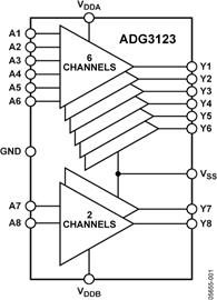
The internal architecture of the device ensures compatibility with logic circuits running from supply voltages within the 2.3 V 5.5 V range. The voltages applied to Pin VDDA, Pin VDDB and Pin VSS set the logic levels available at the outputs on the Y side of the device. Pin VDDA and Pin VDDB set the high output level for Pin Y1 to Pin Y6 and for Pin Y7 to Pin Y8, respectively. The VSS pin sets the low output level for all channels. The ADG3123 can provide output voltages levels down to −24.2 V for a low input level and up to +35 V for a high input logic level. For proper operation, VDDB must always be greater than or equal to VDDA and the voltage between the Pin VSS and Pin VSS should not exceed 35 V.
The low output impedance of the channels guarantees fast rise and fall times even for significant capacitive loads. This feature, combined with low propagation delay and low power consumption, makes the ADG3123 an ideal driver for TFT-LCD panel applications.
The ADG3123 is guaranteed to operate over the −40°C to +85°C temperature range and is available in a compact, 20-lead TSSOP, Pb-free package.
Product Highlights
- Compatible with a wide range of CMOS logic levels.
- High output voltage levels.
- Fast rise and fall times coupled with low propagation delay.
- Ultralow power consumption.
- Compact, 20-lead TSSOP, RoHS-compliant package.
Applications
- Low Voltage to High Voltage Translation
- TFT-LCD Panels
- Piezoelectric Motor Drivers
At least one model within this product family is in production and available for purchase. The product is appropriate for new designs but newer alternatives may exist.


