
- Manufacturer Part Number : AD807A-155BRZ
- Manufacturer : AD
- Description : 155 Mbps, Low Power, Post-Amp/Clock and Data Recovery IC IC
- Series : AD807
- Reference Price : USD 0
- Our Price : We have a better price, contact us by email
- Product Type : Fiber Optic Data
- Function : Clock & Data Recovery/Retiming
- Current Suggest : Not Recommended for New Designs
- Status : Production
- ROHS Status : ROHS Compliant (Lead Free)
- Package Type : 16-Lead SOIC
- Pins : 16
- MFG Package Case : R-16
- Part Type : OTH
- Standard Packing Type : Tube
- Standard Packing Quantity : 48
- Working Temperature : -40 to 85C
- Other Part Number : AD807A-155BRZ
- Shipping methods : DHL FEDEX UPS TNT
- Delivery Time : Ship within 1 day.
- Manufacturer Production time : 6-8 weeks (Normally have stocks)
- Weight : 0.001KG
Contact us to check the best price and real time inventory quantity for AD807A-155BRZ. If you need any more information about AD807A-155BRZ, you can also send us by email. Our email is [email protected], we will reply you in 12 hours.
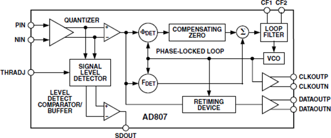
The AD807 provides the receiver functions of data quantization, signal level detect, clock recovery and data retiming for 155 Mbps NRZ data. The device, together with a PIN diode/preamplifier combination, can be used for a highly integrated, low cost, low power SONET OC-3 or SDH STM-1 fiber optic receiver.
The receiver front end signal level detect circuit indicates when the input signal level has fallen below a user adjustable threshold. The threshold is set with a single external resistor. The signal level detect circuit 3 dB optical hysteresis prevents chatter at the signal level detect output.
The PLL has a factory trimmed VCO center frequency and a frequency acquisition control loop that combine to guarantee frequency acquisition without false lock. This eliminates a reliance on external components such as a crystal or a SAW filter, to aid frequency acquisition.
The AD807 acquires frequency and phase lock on input data using two control loops that work without requiring external control. The frequency acquisition control loop initially acquires the frequency of the input data, acquiring frequency lock on random or scrambled data without the need for a preamble. At frequency lock, the frequency error is zero and the frequency detector has no further effect. The phase acquisition control loop then works to ensure that the output phase tracks the input phase. A patented phase detector has virtually eliminated pattern jitter throughout the AD807.
The device VCO uses a ring oscillator architecture and patented low noise design techniques. Jitter is 2.0 degrees rms. This low jitter results from using a fully differential signal architecture, Power Supply Rejection Ratio circuitry and a dielectrically isolated process that provides immunity from extraneous signals on the IC. The device can withstand hundreds of millivolts of power supply noise without an effect on jitter performance.
The user sets the jitter peaking and acquisition time of the PLL by choosing a damping factor capacitor whose value determines loop damping. CCITT G.958 Type A jitter transfer requirements can easily be met with a damping factor of 5 or greater.
Device design guarantees that the clock output frequency will drift by less than 20% in the absence of input data transitions. Shorting the damping factor capacitor, CD, brings the clock output frequency to the VCO center frequency.
The AD807 consumes 140 mW and operates from a single power supply at either +5 V or –5.2 V.
This designates products ADI does not recommend broadly for new designs.


