
- Manufacturer Part Number : ADP5070
- Manufacturer : AD
- Description : 1 A/0.6 A, DC-to-DC Switching Regulator with Independent Positive and Negative Outputs
- Series : ADP5070
- Reference Price : USD 1.752
- Our Price : We have a better price, contact us by email
- Product Type : Switching Regulators
- Function : Step-Up (Boost) Regulators
- Current Suggest : Recommended for New Designs
- Status : Production
- RoHS Status: -
- Voltage: -
- Feature: -
- Package Case: -
- Temperature Range: -
- Packing: Reel/Tray/Tube
- Standard Packing Quantity: -
- Country of Origin: -
- Other Part Number : ADP5070
- Shipping methods : DHL FEDEX UPS TNT
- Delivery Time : Ship within 1 day.
- Manufacturer Production time : 6-8 weeks (Normally have stocks)
- Weight : 0.001KG
Contact us to check the best price and real time inventory quantity for ADP5070. If you need any more information about ADP5070, you can also send us by email. Our email is [email protected], we will reply you in 12 hours.
- Wide input supply voltage range: 2.85 V to 15 V
- Generates well regulated, independently resistor programmable VPOS and VNEG outputs
- Boost regulator to generate VPOS output
- Adjustable positive output to 39 V
- Integrated 1.0 A main switch
- Optional single-ended primary-inductor converter (SEPIC) configuration for automatic step-up/step-down
- Inverting regulator to generate VNEG output
- Adjustable negative output to VIN − 39 V
- Integrated 0.6 A main switch
- True shutdown for both positive and negative outputs
- 1.2 MHz/2.4 MHz switching frequency with optional external frequency synchronization from 1.0 MHz to 2.6 MHz
- Resistor programmable soft start timer
- Slew rate control for lower system noise
- Individual precision enable and flexible start-up sequence control for symmetric start, VPOS first, or VNEG first
- Out-of-phase operation
- UVLO, OCP, OVP, and TSD protection
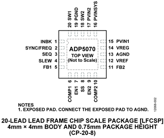
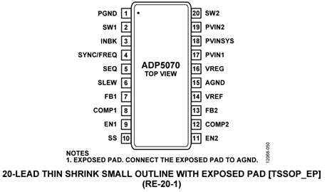
- 4 mm × 4 mm, 20-lead LFCSP and 20-lead TSSOP
- −40°C to +125°C junction temperature range
- Supported by the ADIsimPower tool set
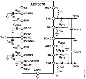
The ADP5070 is a dual high performance dc-to-dc regulator thatgenerates independently regulated positive and negative rails.The input voltage range of 2.85 V to 15 V supports a wide variety ofapplications. The integrated main switch in both regulators enablesgeneration of an adjustable positive output voltage up to +39 Vand a negative output voltage down to −39 V below input voltage.
The ADP5070 operates at a pin selected 1.2 MHz/2.4 MHzswitching frequency. The ADP5070 can synchronize with anexternal oscillator from 1.0 MHz to 2.6 MHz to ease noisefiltering in sensitive applications. Both regulators implementprogrammable slew rate control circuitry for the MOSFETdriver stage to reduce electromagnetic interference (EMI).Flexible start-up sequencing is provided with the options ofmanual enable, simultaneous mode, positive supply first, andnegative supply first.
The ADP5070 includes a fixed internal or resistor programmablesoft start timer to prevent inrush current at power-up. Duringshutdown, both regulators completely disconnect the loads fromthe input supply to provide a true shutdown.
Other key safety features in the ADP5070 include overcurrentprotection (OCP), overvoltage protection (OVP), thermalshutdown (TSD), and input undervoltage lockout (UVLO).The ADP5070 is available in a 20-lead LFCSP or in a 20-leadTSSOP and is rated for a −40°C to +125°C junction temperaturerange.
Applications
- Bipolar amplifiers, ADCs, DACs and multiplexers
- Charge-coupled device (CCD) bias supply
- Optical module supply
- RF power amplifier (PA) bias
This product has been released to the market. The data sheet contains all final specifications and operating conditions. For new designs, ADI recommends utilization of these products.


