
- Manufacturer Part Number : ADRV9008-2W/PCBZ
- Manufacturer : AD
- Description : Quad Buck Regulator Integrated Power Solution IC
- Series : ADP5054
- Reference Price : USD 0
- Our Price : We have a better price, contact us by email
- Product Type : Switching Regulators
- Function : Step-Down (Buck) Regulators
- Current Suggest : Recommended for New Designs
- Status : Production
- ROHS Status : ROHS Compliant (Lead Free)
- Package Type : ADRV9008-1 Tx/ORx Wideband Evaluation Board
- Pins : -
- MFG Package Case : -
- Part Type : EVAL
- Standard Packing Type : -
- Standard Packing Quantity : -
- Working Temperature : -
- Other Part Number : ADRV9008-2W/PCBZ
- Shipping methods : DHL FEDEX UPS TNT
- Delivery Time : Ship within 1 day.
- Manufacturer Production time : 6-8 weeks (Normally have stocks)
- Weight : 0.001KG
Contact us to check the best price and real time inventory quantity for ADRV9008-2W/PCBZ. If you need any more information about ADRV9008-2W/PCBZ, you can also send us by email. Our email is [email protected], we will reply you in 12 hours.
- Wide input voltage range: 4.5 V to 15.5 V
- ±1.5% output accuracy over full temperature range
- 250 kHz to 2 MHz adjustable switching frequency with individual ½× frequency option
- Power regulation
- Channel 1 and Channel 2
- Programmable 2 A/4 A/6 A sync buck regulators with low-side FET drivers
- Channel 3 and Channel 4: 2.5 A sync buck regulators
- Channel 1 and Channel 2
- Flexible parallel operation
- Single 12 A output (Channel 1 and Channel 2 in parallel)
- Single 5 A output (Channel 3 and Channel 4 in parallel)
- Low 1/f noise density
- 40 μV rms at 0.8 VREF for 10 Hz to 100 kHz
- Precision enable with 0.811 V accurate threshold
- Active output discharge switch
- FPWM/PSM mode selection
- Frequency synchronization input or output
- Power-good flag for Channel 1 output
- UVLO, OCP, and TSD protection
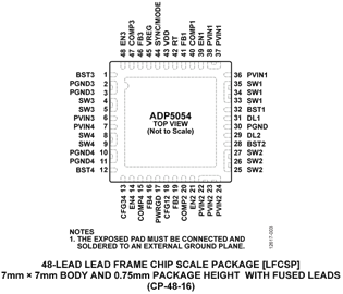
- 48-lead, 7 mm × 7 mm LFCSP
- −40°C to +125°C operational junctional temperature range
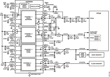
The ADP5054 combines four high performance buck regulators in a 48-lead LFCSP package that meets demanding performance and board space requirements. The device enables direct connection to high input voltages of up to 15.5 V with no preregulators.
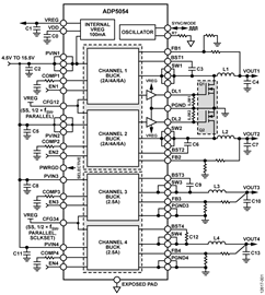
Channel 1 and Channel 2 integrate high-side power metal-oxide semiconductor field effect transistors (MOSFETs ) and low-side MOSFET drivers. External NFETs can be used in low-side power devices to achieve an efficiency optimized solution and to deliver a programmable output current of 2 A, 4 A, or 6 A. Combining Channel 1 and Channel 2 in a parallel configuration provides a single output with up to 12 A of current.
Channel 3 and Channel 4 integrate both high-side and low-side MOSFETs to deliver an output current of 2.5 A. Combining Channel 3 and Channel 4 in a parallel configuration can provide a single output with up to 5 A of current.
The switching frequency of the ADP5054 can be programmed or synchronized to an external clock from 250 kHz to 2 MHz, and an individual ½× frequency configuration is available for each channel.
The ADP5054 contains an individual precision enable pin on each channel for easy power-up sequencing. The internal low 1/f noise reference is implemented in the ADP5054 for noise sensitive applications.
Applications
- FPGA and processor applications
- Small cell base stations
- Security and surveillance
- Medical applications
This product has been released to the market. The data sheet contains all final specifications and operating conditions. For new designs, ADI recommends utilization of these products.


