
- Manufacturer Part Number : LTC3256IMSE#PBF
- Manufacturer : AD
- Description : Wide VIN Range Dual Output 350mA Step-Down Charge Pump with Watchdog Timer IC
- Series : LTC3256
- Reference Price : USD 2.68
- Our Price : We have a better price, contact us by email
- Product Type : Inductorless (Charge Pump) DC/DC Converters
- Function : High Voltage Charge Pumps
- Current Suggest : Recommended for New Designs
- Status : Production
- ROHS Status : ROHS Compliant (Lead Free)
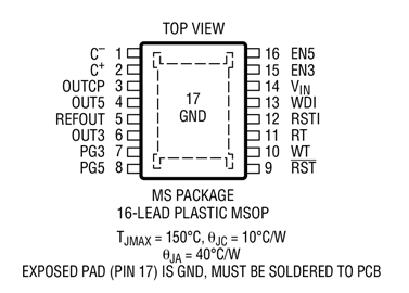
- Package Type : 16-Lead MSOP w/ EP
- Pins : 16
- MFG Package Case : 05-08-1667
- Part Type : OTH
- Standard Packing Type : Tube
- Standard Packing Quantity : 37
- Working Temperature : -40 to 125C
- Other Part Number : LTC3256IMSE#PBF
- Shipping methods : DHL FEDEX UPS TNT
- Delivery Time : Ship within 1 day.
- Manufacturer Production time : 6-8 weeks (Normally have stocks)
- Weight : 0.001KG
Contact us to check the best price and real time inventory quantity for LTC3256IMSE#PBF. If you need any more information about LTC3256IMSE#PBF, you can also send us by email. Our email is [email protected], we will reply you in 12 hours.
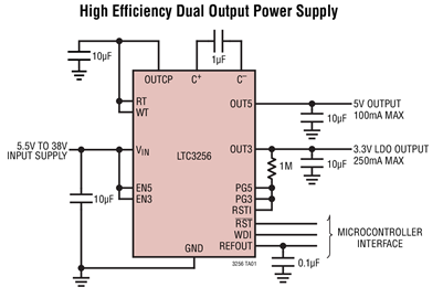
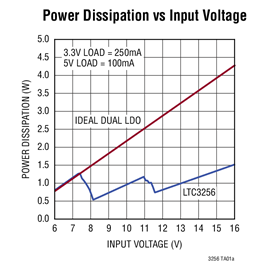
The LTC3256 is a wide input range switched capacitor step-down DC/DC converter that produces two regulated outputs: a 5V output via direct connection to the charge pump output, and a 3.3V output via a low dropout (LDO) linear post-regulator. The device provides up to 350mA of total output current. At 12V VIN and maximum load on both outputs, power dissipation is reduced by over 2W compared to a dual LDO regulator solution.
The LTC3256 maximizes efficiency by running the charge pump in 2:1 mode over as wide an operating range as pos- sible, and automatically switches to 1:1 mode as needed due to VIN and load conditions. Controlled input current and switching slew rates minimize conducted and radiated EMI. An integrated watchdog timer, independent power good outputs and reset input ensure reliable system operation and fault monitoring. A buffered 1.1V reference output enables system self-testing for safety critical applications.
The LTC3256 has numerous safety features including overcurrent fault protection, overtemperature protection and tolerance of 38V input transients. The LTC3256 is available in a thermally enhanced 16-lead MSOP plastic package with exposed pad (MSE16).
Applications
- Automotive ECU/CAN Transceiver Supplies
- Industrial/Telecom Housekeeping Supplies
- Low Power 12V to 5V and 3.3V Conversion
This product has been released to the market. The data sheet contains all final specifications and operating conditions. For new designs, ADI recommends utilization of these products.


