
- Manufacturer Part Number : LTC3290
- Manufacturer : AD
- Description : High Voltage Boost Charge Pump
- Series : LTC3290
- Reference Price : USD 1.864
- Our Price : We have a better price, contact us by email
- Product Type : Inductorless (Charge Pump) DC/DC Converters
- Function : Regulated Step-Up Charge Pumps
- Current Suggest : Recommended for New Designs
- Status : Production
- RoHS Status: -
- Voltage: -
- Feature: -
- Package Case: -
- Temperature Range: -
- Packing: Reel/Tray/Tube
- Standard Packing Quantity: -
- Country of Origin: -
- Other Part Number : LTC3290
- Shipping methods : DHL FEDEX UPS TNT
- Delivery Time : Ship within 1 day.
- Manufacturer Production time : 6-8 weeks (Normally have stocks)
- Weight : 0.001KG
Contact us to check the best price and real time inventory quantity for LTC3290. If you need any more information about LTC3290, you can also send us by email. Our email is [email protected], we will reply you in 12 hours.
- Wide Input Range: 4.5V to 55V VIN/VAUX
- Reverse Input Protection to –55V
- Split Input Supplies for High Efficiency Boost Ratios
- IOUT Up to 50mA
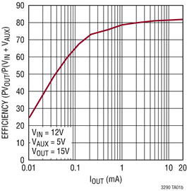
- 15µA VIN Quiescent Current
- 1µA VAUX Quiescent Current
- Stable with Ceramic Capacitors
- Short-Circuit/Thermal Protection
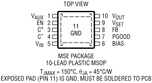
- Thermally Enhanced 10-Pin MSOP Package
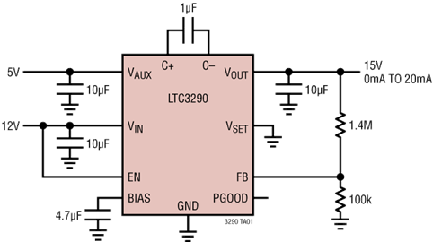
The LTC3290 is a high voltage boost charge pump with a wide 4.5V to 55V input voltage range that can deliver up to 50mA of output current.
When the VSET pin is grounded, the LTC3290 operates as a standard boost charge pump, boosting the VOUT output to a maximum of the sum of the VIN and VAUX input supplies. An external resistor divider can be used on the VOUT, FB and GND pins to set the output voltage to any value between 1V and VIN + VAUX with hysteretic Burst Mode operation.
Alternatively, the device can be configured in a VIN tracking mode, in which the VOUT pin regulates at a fixed offset above the VIN pin. The offset voltage is programmed with external resistors, one from the VOUT to the VSET pin and the other from the FB pin to GND. The maximum output voltage is limited to VIN + VAUX.
The LTC3290 is available in a thermally enhanced 10-pin MSOP package.
Applications
- High Efficiency General Purpose High Voltage Boost Supplies
- High Side N-FET Driver
- Industrial/Automotive Power Switching
- VIN Tracking Supply
This product has been released to the market. The data sheet contains all final specifications and operating conditions. For new designs, ADI recommends utilization of these products.


