
- Manufacturer Part Number : ADUC7128
- Manufacturer : AD
- Description : Precision Analog Microcontroller ARM7TDMI® MCU with 12-Bit ADC and DDS DAC
- Series : ADUC7128
- Reference Price : USD 5.792
- Our Price : We have a better price, contact us by email
- Product Type : Microcontrollers
- Function : ARM7 Core Products
- Current Suggest : Production
- Status : Production
- RoHS Status: -
- Voltage: -
- Feature: -
- Package Case: -
- Temperature Range: -
- Packing: Reel/Tray/Tube
- Standard Packing Quantity: -
- Country of Origin: -
- Other Part Number : ADUC7128
- Shipping methods : DHL FEDEX UPS TNT
- Delivery Time : Ship within 1 day.
- Manufacturer Production time : 6-8 weeks (Normally have stocks)
- Weight : 0.001KG
Contact us to check the best price and real time inventory quantity for ADUC7128. If you need any more information about ADUC7128, you can also send us by email. Our email is [email protected], we will reply you in 12 hours.
- Multi-Channel, 12-bit, 1MSPS ADC
Up to 14 analog-to-digital converter (ADC) channels
Fully differential and single-ended modes
0 to VREF Analog Input Range - 10-bit digital-to-analog converter (DAC)
32-bit 21 MHz direct digital synthesis (DDS)
Current-to-Voltage (I/V) Conversion
Integrated second-order low-pass filter (LPF)
DDS Input to DAC
100 Ω line driver - On-Chip Voltage Reference
- On-Chip Temperature Sensor (±3°C)
- Voltage Comparator
- ARM7TDMI Core, 16/32-bit RISC architecture
- JTAG Port supports code download and debug
- External Watch crystal/ Clock Source
41.78 MHz PLL with 8 way Programmable Divider
Optional Trimmed On-Chip Oscillator
- 126 kB Flash/EE memory, 8 kB SRAM
- In-Circuit Download, JTAG based Debug
- Software triggered in-circuit re-programmability
- 2 x UART, 2 x I2C® and SPI Serial I/O
- Up to 40-pin GPIO port
- 5 X General Purpose Timers
- Wake-up and watchdog timers (WDT)
- Power Supply Monitor
- 16-bit PWM generator
- Quadrature Encoder
- Programmable Logic Array (PLA)
- Specified for 3V operation
- Active Mode:
11 mA (@ 5.22 MHz)
45 mA (@ 41.78 MHz)
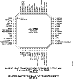
- 64-lead 9 mm × 9 mm LFCSP package, −40°C to 125°C
- 64-lead LQFP, −40°C to +125°C
- 80-lead LQFP, −40°C to +125°C
- Low-Cost QuickStart Development System
- Full Third-Party Support
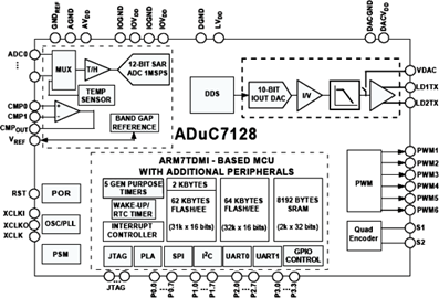
The ADC consists of up to 14 single-ended inputs. The ADC can operate in single-ended or differential input modes. The ADC input voltage is 0 to VREF. Low drift band gap reference, temperature sensor, and voltage comparator complete the ADC peripheral set.
The ADuC7128/ADuC7129 integrate a differential line driver output. This line driver transmits a sine wave whose values are calculated by an on-chip DDS or a voltage output determined by the DACDAT MMR.
The devices operate from an on-chip oscillator and PLL, generating an internal high frequency clock of 41.78 MHz. This clock is routed through a programmable clock divider from which the MCU core clock operating frequency is generated.
The microcontroller core is an ARM7TDMI®, 16-/32-bit reduced instruction set computer (RISC), offering up to 41 MIPS peak performance. There are 126 kB of nonvolatile Flash/EE provided on-chip, as well as 8 kB of SRAM. The ARM7TDMI core views all memory and registers as a single linear array.
On-chip factory firmware supports in-circuit serial download via the UART serial interface port, and nonintrusive emulation is also supported via the JTAG interface. These features are incorporated into a low cost QuickStart™ development system supporting this MicroConverter® family.
The parts operate from 3.0 V to 3.6 V and are specified over an industrial temperature range of −40°C to +125°C. When operating at 41.78 MHz, the power dissipation is 135 mW. The line driver output, if enabled, consumes an additional 30 mW.
At least one model within this product family is in production and available for purchase. The product is appropriate for new designs but newer alternatives may exist.


