
- Manufacturer Part Number : AD8312-EVALZ
- Manufacturer : AD
- Description : 50 MHz TO 3.5 GHz, 45 dB RF Detector IC
- Series : AD8312
- Reference Price : USD 0
- Our Price : We have a better price, contact us by email
- Product Type : RF Power Detectors
- Function : Log Detectors
- Current Suggest : Recommended for New Designs
- Status : Production
- ROHS Status : ROHS Compliant (Lead Free)
- Package Type : Evaluation Board
- Pins : -
- MFG Package Case : -
- Part Type : EVAL
- Standard Packing Type : -
- Standard Packing Quantity : -
- Working Temperature : -
- Other Part Number : AD8312-EVALZ
- Shipping methods : DHL FEDEX UPS TNT
- Delivery Time : Ship within 1 day.
- Manufacturer Production time : 6-8 weeks (Normally have stocks)
- Weight : 0.001KG
Contact us to check the best price and real time inventory quantity for AD8312-EVALZ. If you need any more information about AD8312-EVALZ, you can also send us by email. Our email is [email protected], we will reply you in 12 hours.
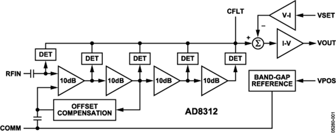
The AD8312 is a complete, low cost subsystem for the measurement of RF signals in the frequency range of 50 MHz to 3.5 GHz. It has a typical dynamic range of 45 dB and is intended for use in a wide variety of cellular handsets and other wireless devices. It provides a wider dynamic range and better accuracy than possible using discrete diode detectors. In particular, its temperature stability is excellent over the full operating range of −40°C to +85°C.
Its high sensitivity allows measurement at low power levels, thus reducing the amount of power that needs to be coupled to the detector. It is essentially a voltage-responding device, with a typical signal range of 1.25 mV to 224 mV rms or −45 dBm to 0 dBm, referencing 50 Ω.
For convenience, the signal is internally ac-coupled, using a 5 pF capacitor to a load of 3 kΩ in shunt with 1.3 pF. This high-pass coupling, with a corner at approximately 16 MHz, determines the lowest operating frequency. Therefore, the source may be dc grounded.
The AD8312 output, VOUT, increases from close to ground to about 1.2 V because the input signal level increases from 1.25 mV to 224 mV. A capacitor may be connected between the VOUT and CFLT pins when it is desirable to increase the time interval over which averaging of the input waveform occurs.
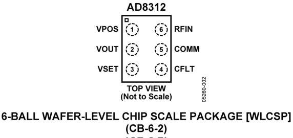
The AD8312 is available in a 6-ball, 1.0 mm × 1.5 mm, wafer-level chip scale package and consumes 4.2 mA from a 2.7 V to 5.5 V supply.
Applications
- Cellular handsets (GSM, CDMA, WCDMA)
- RSSI and TSSI for wireless terminal devices
- Transmitter power measurement
This product has been released to the market. The data sheet contains all final specifications and operating conditions. For new designs, ADI recommends utilization of these products.


