
- Manufacturer Part Number : AD9371BBCZ
- Manufacturer : AD
- Description : Integrated, Dual RF Transceiver with Observation Path IC
- Series : AD9371
- Reference Price : USD 196
- Our Price : We have a better price, contact us by email
- Product Type : RF Integrated Transmitters, Receivers, & Transceivers
- Function : Wideband Transceiver IC
- Current Suggest : Recommended for New Designs
- Status : Production
- ROHS Status : ROHS Compliant (Lead Free)
- Package Type : 196-Ball CSPBGA (12mm x 12mm x 1.27mm)
- Pins : 196
- MFG Package Case : BC-196-12
- Part Type : OTH
- Standard Packing Type : Tray
- Standard Packing Quantity : 189
- Working Temperature : -40 to 85C
- Other Part Number : AD9371BBCZ
- Shipping methods : DHL FEDEX UPS TNT
- Delivery Time : Ship within 1 day.
- Manufacturer Production time : 6-8 weeks (Normally have stocks)
- Weight : 0.001KG
Contact us to check the best price and real time inventory quantity for AD9371BBCZ. If you need any more information about AD9371BBCZ, you can also send us by email. Our email is [email protected], we will reply you in 12 hours.
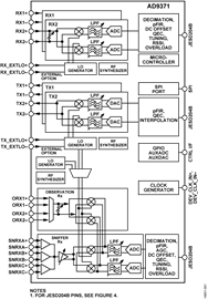
The AD9371 is a highly integrated, wideband RF transceiveroffering dual channel transmitters and receivers, integrated synthesizers, and digital signal processing functions. The ICdelivers a versatile combination of high performance and low power consumption required by 3G/4G micro and macro BTSequipment in both FDD and TDD applications. The AD9371operates from 300 MHz to 6000 MHz, covering most of the licensed and unlicensed cellular bands. The IC supports receiver bandwidths up to 100 MHz. It also supports observation receiver and transmit synthesis bandwidths up to 250 MHz to accommodate digital correction algorithms.
The transceiver consists of wideband direct conversion signalpaths with state-of-the-art noise figure and linearity. Each complete receiver and transmitter subsystem includes dc offset correction, quadrature error correction (QEC), and programmable digitalfilters, eliminating the need for these functions in the digitalbaseband. Several auxiliary functions such as an auxiliary analog-to-digital converter (ADC), auxiliary digital-to-analog converters (DACs), and general-purpose input/outputs (GPIOs) are integratedto provide additional monitoring and control capability.
An observation receiver channel with two inputs is included to monitor each transmitter output and implement interference mitigation and calibration applications. This channel also connects to three sniffer receiver inputs that can monitor radio activity in different bands.
The high speed JESD204B interface supports lane rates up to 6144 Mbps. Four lanes are dedicated to the transmitters and four lanes are dedicated to the receiver and observation receiver channels.
The fully integrated phase-locked loops (PLLs) provide high performance, low power fractional-N frequency synthesis forthe transmitter, the receiver, the observation receiver, and theclock sections. Careful design and layout techniques provide theisolation demanded in high performance base station applications.All voltage controlled oscillator (VCO) and loop filter components are integrated to minimize the external component count.
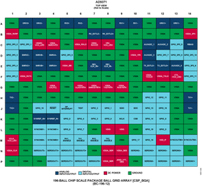
A 1.3 V supply is required to power the core of the AD9371, anda standard 4-wire serial port controls it. Other voltage supplies provide proper digital interface levels and optimize transmitterand auxiliary converter performance. The AD9371 is packaged in a12 mm × 12 mm, 196-ball chip scale ball grid array (CSP_BGA).
Applications
- 3G/4G micro and macro base stations (BTS)
- 3G/4G multicarrier picocells
- FDD and TDD active antenna systems
- Microwave, nonline of sight (NLOS) backhaul systems
This product has been released to the market. The data sheet contains all final specifications and operating conditions. For new designs, ADI recommends utilization of these products.


