
- Manufacturer Part Number : ADL5367ACPZ-R7
- Manufacturer : AD
- Description : 500 MHz TO 1700 MHz Balanced Mixer, LO Buffer and RF Balun IC
- Series : ADL5367
- Reference Price : USD 4.792
- Our Price : We have a better price, contact us by email
- Product Type : RF Mixers
- Function : Single, Double & Triple Balanced Mixers
- Current Suggest : Last Time Buy
- Status : Last Time Buy
- ROHS Status : ROHS Compliant (Lead Free)
- Package Type : 20-Lead LFCSP (5mm x 5mm x 0.75mm w/ EP)
- Pins : 20
- MFG Package Case : CP-20-9
- Part Type : REEL
- Standard Packing Type : Reel
- Standard Packing Quantity : 1500
- Working Temperature : -40 to 85C
- Other Part Number : ADL5367ACPZ-R7
- Shipping methods : DHL FEDEX UPS TNT
- Delivery Time : Ship within 1 day.
- Manufacturer Production time : 6-8 weeks (Normally have stocks)
- Weight : 0.001KG
Contact us to check the best price and real time inventory quantity for ADL5367ACPZ-R7. If you need any more information about ADL5367ACPZ-R7, you can also send us by email. Our email is [email protected], we will reply you in 12 hours.
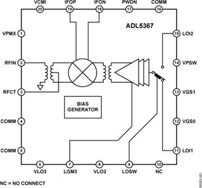
The ADL5367 uses a highly linear, doubly balanced passivemixer core along with integrated RF and LO balancing circuitryto allow for single-ended operation. The ADL5367 incorporatesan RF balun, allowing optimal performance over a 500 MHz to1700 MHz RF input frequency range. Performance is optimized forRF frequencies from 500 MHz to 1200 MHz using a high-side LOand for RF frequencies from 900 MHz to 1700 MHz using alow-side LO. The balanced passive mixer arrangement providesgood LO to RF leakage, typically better than −35 dBm, andexcellent intermodulation performance. The balanced mixercore also provides extremely high input linearity, allowing thedevice to be used in demanding cellular applications where inbandblocking signals may otherwise result in the degradationof dynamic performance. A high linearity IF buffer amplifierfollows the passive mixer core to yield a typical power conversionloss of 7.7 dB and can be used with a wide range of outputimpedances.
The ADL5367 provides two switched LO paths that can beused in TDD applications where it is desirable to rapidly switchbetween two local oscillators. LO current can be externally setusing a resistor to minimize dc current commensurate with thedesired level of performance. For low voltage applications, theADL5367 is capable of operation at voltages down to 3.3 V withsubstantially reduced current. Under low voltage operation, anadditional logic pin is provided to power down (<200 µA) thecircuit when desired.
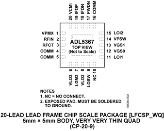
The ADL5367 is fabricated using a BiCMOS high performanceIC process. The device is available in a 5 mm × 5 mm, 20-leadLFCSP and operates over a −40°C to +85°C temperature range.An evaluation board is also available.
Applications
- Cellular base station receivers
- Transmit observation receivers
- Radio link downconverters
All products in this family will be obsolete soon. Please contact ADI Sales or Distributors to arrange for final purchases and read our Obsolescence Information to review the time periods for placing final orders and receiving final shipments.


