
- Manufacturer Part Number : ADL5519ACPZ-R7
- Manufacturer : AD
- Description : 1 MHz TO 10 GHz, 62 dB Dual Log Detector / Controller IC
- Series : ADL5519
- Reference Price : USD 4.032
- Our Price : We have a better price, contact us by email
- Product Type : RF Power Detectors
- Function : Log Detectors
- Current Suggest : Recommended for New Designs
- Status : Production
- ROHS Status : ROHS Compliant (Lead Free)
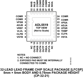
- Package Type : 32-Lead LFCSP (5mm x 5mm x 0.75mm w/ EP)
- Pins : 32
- MFG Package Case : CP-32-21
- Part Type : REEL
- Standard Packing Type : Reel
- Standard Packing Quantity : 1500
- Working Temperature : -40 to 125C
- Other Part Number : ADL5519ACPZ-R7
- Shipping methods : DHL FEDEX UPS TNT
- Delivery Time : Ship within 1 day.
- Manufacturer Production time : 6-8 weeks (Normally have stocks)
- Weight : 0.001KG
Contact us to check the best price and real time inventory quantity for ADL5519ACPZ-R7. If you need any more information about ADL5519ACPZ-R7, you can also send us by email. Our email is [email protected], we will reply you in 12 hours.
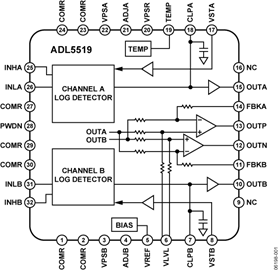
The ADL5519 is a dual-demodulating logarithmic amplifier that incorporates two AD8317s. It can accurately convert an RF input signal into a corresponding decibel-scaled output. The ADL5519 provides accurately scaled, independent, logarithmic output voltages for both RF measurement channels. The device has two additional output ports, OUTP and OUTN, that provide the measured differences between the OUTA and OUTB channels. The on-chip channel matching makes the log amp outputs insensitive to temperature and process variations.
The temperature sensor pin provides a scaled voltage that is proportional to the temperature over the operating temperature range of the device.
The ADL5519 maintains accurate log conformance for signals from 1 MHz to 8 GHz and provides useful operation to 10 GHz. The ±3 dB dynamic range is typically 62 dB and has a ±1 dB dynamic range of >50 dB (re: 50 Ω). The ADL5519 has a response time of 6 ns/8 ns (fall time/rise time) that enables RF burst detection to a pulse rate of greater than 50 MHz. The device provides unprecedented logarithmic intercept stability vs. ambient temperature conditions. A supply of 3.3 V to 5.5 V is required to power the device. Current consumption is typically 60 mA, and it decreases to less than 1 mA when the device is disabled.
The device is capable of supplying four log amp measurements simultaneously. Linear-in-dB measurements are provided at OUTA and OUTB with conveniently scaled slopes of −22 mV/dB. The log amp difference between OUTA and OUTB is available as differential or single-ended signals at OUTP and OUTN. An optional voltage applied to VLVL provides a common-mode reference level to offset OUTP and OUTN above ground. The broadband output pins can support many system solutions.
Any of the ADL5519 output pins can be configured to provide a control voltage to a variable gain amplifier (VGA). Special attention has been paid to minimize the broadband noise of the output pins so that they can be used for controller applications.
The ADL5519 is fabricated on a SiGe bipolar IC process and is available in a 5 mm × 5 mm, 32-lead LFCSP with an operating temperature range of −40°C to +125°C.
Applications
- RF transmitter power amplifier linearization and gain/power control
- Power monitoring in radio link transmitters
- Dual-channel wireless infrastructure radios
- Antenna VSWR monitor
- RSSI measurement in base stations, WLAN, WiMAX, radar
This product has been released to the market. The data sheet contains all final specifications and operating conditions. For new designs, ADI recommends utilization of these products.


