
- Manufacturer Part Number : ADL6010R703LSH6
- Manufacturer : AD
- Description : Aerospace ADL6010S Fast Responding, 45 dB Range, 0.5 GHz TO 43.5 GHz Envelope Detector IC
- Series : ADL6010S
- Reference Price : USD 0
- Our Price : We have a better price, contact us by email
- Product Type : RF Power Detectors
- Function : Envelope Detectors & Peak Detectors
- Current Suggest : Recommended for New Designs
- Status : Contact ADI
- ROHS Status : ROHS Compliant (Lead Free)
- Package Type : CER LDLESS CHIP W/HEATSINK
- Pins : 16
- MFG Package Case : X
- Part Type : OTH
- Standard Packing Type : Tube
- Standard Packing Quantity : 0
- Working Temperature :
- Other Part Number : ADL6010R703LSH6
- Shipping methods : DHL FEDEX UPS TNT
- Delivery Time : Ship within 1 day.
- Manufacturer Production time : 6-8 weeks (Normally have stocks)
- Weight : 0.001KG
Contact us to check the best price and real time inventory quantity for ADL6010R703LSH6. If you need any more information about ADL6010R703LSH6, you can also send us by email. Our email is [email protected], we will reply you in 12 hours.
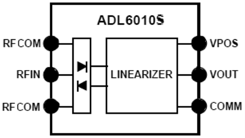
The ADL6010S is a versatile, broadband envelope detector covering the microwave spectrum. It provides state-of-the-art accuracy with very low power consumption (8 mW) in a RF hermetic package. The output is a baseband voltage proportional to the instantaneous amplitude of the radio frequency (RF) input signal. It exhibits minimal slope variation of the RF input to envelope output transfer function from 0.5 GHz to 43.5 GHz.
The detector cell uses a proprietary eight Schottky diode array followed by a novel linearizer circuit that creates a linear voltmeter with an overall scaling factor (or transfer gain) of nominally ×2.2 relative to the voltage amplitude of the input.
Although the ADL6010S is not inherently a power responding device, it remains convenient to specify the input in this way. Thus, the permissible input power, relative to a 50 Ω source input impedance, ranges from −30 dBm to +15 dBm. The corresponding input voltage amplitudes of 11.2 mV to 1.8 V generate quasi-dc outputs from about 25 mV to 4 V above common (COMM).
A subtle aspect of the balanced detector topology is that no even-order distortion, caused by nonlinear source loading, occurs at the input. This is an important benefit in applications where a low ratio coupler is used to extract a signal sample and is a significant improvement over traditional diode detectors.
The output response accuracy is insensitive to variation in the supply voltage, which can range from 4.75 V to 5.25 V. The ultralow power dissipation contributes to its long-term stability.
The ADL6010S is specified for operation from −55°C to +125°C. Both are available in a 16-lead, 6 mm × 6 mm LSH6 hermetic square leadless RF Via Chip Carrier package.
Applications
- Power Detector
- Input Voltage Level Correction
- AGC
- Quadrature Error Correction
- RF Power Amplifier Efficiency Enhancement
This product has been released to the market. The data sheet contains all final specifications and operating conditions. For new designs, ADI recommends utilization of these products.


