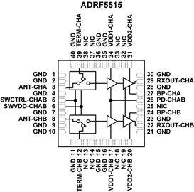

- Manufacturer Part Number : ADRF5515
- Manufacturer : AD
- Description : Dual-Channel, 3.4 GHz to 3.8 GHz 20 W Receiver Front End
- Series : ADRF5515
- Reference Price : USD 0
- Our Price : We have a better price, contact us by email
- Product Type : RF Switches
- Function : RF Front End ICs
- Current Suggest : Pre-Release
- Status : Pre-Release
- RoHS Status: -
- Voltage: -
- Feature: -
- Package Case: -
- Temperature Range: -
- Packing: Reel/Tray/Tube
- Standard Packing Quantity: -
- Country of Origin: -
- Other Part Number : ADRF5515
- Shipping methods : DHL FEDEX UPS TNT
- Delivery Time : Ship within 1 day.
- Manufacturer Production time : 6-8 weeks (Normally have stocks)
- Weight : 0.001KG
Contact us to check the best price and real time inventory quantity for ADRF5515. If you need any more information about ADRF5515, you can also send us by email. Our email is [email protected], we will reply you in 12 hours.
- Integrated dual-channel RF front end
- 2-stage LNA and high power silicon SPDT switch
- On-chip bias and matching
- Single supply operation
- Gain
- High gain mode: 33 dB typical at 3.6 GHz
- Low gain mode: 16 dB typical at 3.6 GHz
- Low noise figure
- High gain mode: 1.0 dB typical at 3.6 GHz
- Low gain mode: 1.0 dB typical at 3.6 GHz
- High isolation
- RXOUT-CHA and RXOUT-CHB: 45 dB typical
- TERM-CHA and TERM-CHB: 60 dB typical
- Low insertion loss: 0.45 dB typical at 3.6 GHz
- High power handling at TCASE = 105°C
- Full lifetime
- LTE average power (9 dB PAR): 43 dBm
- Single event (<10 sec operation)
- LTE average power (9 dB PAR): TBD
- Full lifetime
- High OIP3: 32 dBm typical
- Power-down mode and low gain mode for LNA
- Low supply current
- High gain mode: 86 mA typical at 5V
- Low gain mode: 36 mA typical at 5V
- Power-down mode: 12 mA typical at 5V
- Positive logic control
- 6 mm × 6 mm, 40-lead LFCSP package
- Pin compatible with the ADRF5545A, 10 W version
The ADRF5515 is a dual-channel, integrated radio frequency (RF), front-end multichip module designed for time division duplexing (TDD) applications that operates from 3.4 GHz to 4.0 GHz. The ADRF5515 is configured in dual channels with a cascading two-stage low noise amplifier (LNA) and a high power silicon single-pole, double-throw (SPDT) switch.
In high gain mode, the cascaded two-stage LNA and switch offer a low noise figure (NF) of 1.0 dB and a high gain of 33 dB at 3.6 GHz with an output third-order intercept point (OIP3) of 32 dBm (typical). In low gain mode, one stage of the two-stage LNA is in bypass, providing 16 dB of gain at a lower current of 36 mA. In power-down mode, the LNAs are turned off and the device draws 12 mA.
In transmit operation, when RF inputs are connected to a termination pin (TERM-CHA or TERM-CHB), the switch provides a low insertion loss of 0.45 dB and handles long-term evolution (LTE) average power (9 dB peak to average ratio (PAR)) of 43 dBm for full lifetime operation.
The ADRF5515 is pin-compatible with the ADRF5545A, 10W version, which operates from 2.4 GHz to 4.2 GHz.
The ADRF5515 does not require any matching components at the RF ports that are internally matched to 50 Ω. ANT and TERM ports are also internally ac-coupled. Therefore, only RX ports require external dc blocking capacitors.
The device comes in an RoHS compliant, compact, 6 mm × 6 mm, 40-lead LFCSP package.
Applications
- Wireless infrastructure
- TDD massive multiple input and multiple output and active antenna systems
- TDD-based communications systems
This product is new and engineering validation may still be underway. Quantities may be limited and design specifications may change while we ready the product for release to production.


