
- Manufacturer Part Number : ADRV9008BBCZ-1
- Manufacturer : AD
- Description : Integrated Dual RF Receiver IC
- Series : ADRV9008-1
- Reference Price : USD 168
- Our Price : We have a better price, contact us by email
- Product Type : RF Integrated Transmitters, Receivers, & Transceivers
- Function : Wideband Transceiver IC
- Current Suggest : Recommended for New Designs
- Status : Production
- ROHS Status : ROHS Compliant (Lead Free)
- Package Type : 196-Ball CSPBGA (12mm x 12mm)
- Pins : 196
- MFG Package Case : BC-196-13
- Part Type : OTH
- Standard Packing Type : Tray
- Standard Packing Quantity : 189
- Working Temperature : -40 to 85C
- Other Part Number : ADRV9008BBCZ-1
- Shipping methods : DHL FEDEX UPS TNT
- Delivery Time : Ship within 1 day.
- Manufacturer Production time : 6-8 weeks (Normally have stocks)
- Weight : 0.001KG
Contact us to check the best price and real time inventory quantity for ADRV9008BBCZ-1. If you need any more information about ADRV9008BBCZ-1, you can also send us by email. Our email is [email protected], we will reply you in 12 hours.
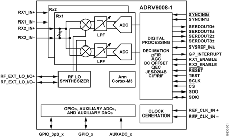
The receive path consists of two independent, wide bandwidth (BW), direct conversion receivers with state-of-the-art dynamic range. The complete receive subsystem includes automatic and manual attenuation control, dc offset correction, quadrature error correction (QEC), and digital filtering, eliminating the need for these functions in the digital baseband. RF front-end control and several auxiliary functions such as analog-to-digital converters (ADCs), digital-to-analog converters (DACs), and general-purpose input/outputs (GPIOs) for the power amplifier (PA) are also integrated.
In addition to automatic gain control (AGC), the ADRV9008-1 also features flexible external gain control modes, allowing significant flexibility in setting system level gain dynamically.
The received signals are digitized with a set of four high dynamic range, continuous time, sigma-delta (Σ-Δ) ADCs that provide inherent antialiasing. The combination of the direct conversion architecture, which does not suffer from out of band image mixing, and the lack of aliasing relaxes the requirements of the RF filters compared to traditional intermediate frequency (IF) receivers.
The fully integrated phase-locked loop (PLL) provides high per-formance, low power, fractional-N, RF synthesis for the receiver signal paths. An additional synthesizer generates the clocks needed for the converters, digital circuits, and the serial interface. A multi-chip synchronization mechanism synchronizes the phase of the RF local oscillator (LO) and baseband clocks between multiple ADRV9008-1 chips. Precautions are taken to provide the isolation required in high performance base station applications. All voltage controlled oscillators (VCOs) and loop filter components are integrated.
The high speed JESD204B interface supports up to 12.288 Gbps lane rates, resulting in two lanes per transmitter and a single lane per receiver in the widest bandwidth mode. The interface also supports interleaved mode for lower bandwidths, reducing the total number of high speed data interface lanes to one. Both fixed and floating point data formats are supported. The floating point format allows internal AGC to be invisible to the demodulator device.
The core of the ADRV9008-1 can be powered directly from 1.3 V and 1.8 V regulators and is controlled via a standard 4-wire serial port. Comprehensive power-down modes are included to mini-mize power consumption during normal use. The ADRV9008-1 is packaged in a 12 mm × 12 mm, 196-ball chip scale ball grid array (CSP_BGA).
Applications
- 3G, 4G, and 5G FDD, macrocell base stations
- Wide band active antenna systems
- Massive multiple input, multiple output (MIMO)
- Phased array radar
- Electronic warfare
- Military communications
- Portable test equipment
This product has been released to the market. The data sheet contains all final specifications and operating conditions. For new designs, ADI recommends utilization of these products.


