
- Manufacturer Part Number : ADRV9008-2W/PCBZ
- Manufacturer : AD
- Description : Integrated Dual RF Transmitter and Observation Receiver IC
- Series : ADRV9008-2
- Reference Price : USD 0
- Our Price : We have a better price, contact us by email
- Product Type : RF Integrated Transmitters, Receivers, & Transceivers
- Function : Wideband Transceiver IC
- Current Suggest : Recommended for New Designs
- Status : Production
- ROHS Status : ROHS Compliant (Lead Free)
- Package Type : ADRV9008-1 Tx/ORx Wideband Evaluation Board
- Pins : -
- MFG Package Case : -
- Part Type : EVAL
- Standard Packing Type : -
- Standard Packing Quantity : -
- Working Temperature : -
- Other Part Number : ADRV9008-2W/PCBZ
- Shipping methods : DHL FEDEX UPS TNT
- Delivery Time : Ship within 1 day.
- Manufacturer Production time : 6-8 weeks (Normally have stocks)
- Weight : 0.001KG
Contact us to check the best price and real time inventory quantity for ADRV9008-2W/PCBZ. If you need any more information about ADRV9008-2W/PCBZ, you can also send us by email. Our email is [email protected], we will reply you in 12 hours.
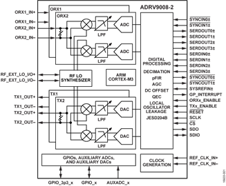
The ADRV9008-2 is a highly integrated, RF agile transmit subsystem offering dual channel transmitters, observation path receiver, integrated synthesizers, and digital signal processing functions. The IC delivers a versatile combination of high performance and low power consumption demanded by 2G, 3G and 4G macro-cell base stations, and active antenna, applications.
The transmitters use an innovative direct conversion modulator that achieves multi-carrier macro-base-station quality performance and very low power. In 3G/4G mode, the maximum large-signal bandwidth is 200MHz. In MC-GSM mode, which has higher in-band SFDR, the maximum large-signal bandwidth is 75MHz.
The observation path consists of a wide bandwidth direct-conversion receiver with state-of-the-art dynamic range. The complete receive subsystem includes dc offset correction, quadrature correction, and digital filtering thus eliminating the need for these functions in the digital baseband. Several auxiliary functions such as ADCs, DACs, and GPIOs for PA and RF-front-end control are also integrated.
The fully integrated phase locked loops (PLLs) provide high performance, low power fractional-N RF frequency synthesis for the transmitter and receiver sections. An additional synthesizer is used to generate the clocks needed for the converters, digital circuits, and the serial interface. Special precautions have been taken to provide the isolation demanded in high performance base station applications. All VCO and loop filter components are integrated.
The high-speed JESD204B interface supports up to 12.288 Gbps lane rates resulting in two lanes per transmitter in the widest bandwidth mode and two lanes for the observation path receiver in the widest bandwidth mode.
The core of the ADRV9008-2 can be powered directly from 1.3 V and 1.8 V regulators and is controlled via a standard 4 wire serial port. Comprehensive power-down modes are included to minimize power consumption in normal use. The ADRV9008-2 is packaged in a 12mm × 12 mm, 196-ball chip scale ball grid array (CSP_BGA).
This product has been released to the market. The data sheet contains all final specifications and operating conditions. For new designs, ADI recommends utilization of these products.


