
- Manufacturer Part Number : ADRV9026
- Manufacturer : AD
- Description : Integrated, Quad RF Transceiver with Observation Path
- Series : ADRV9026
- Reference Price : USD 552
- Our Price : We have a better price, contact us by email
- Product Type : RF Integrated Transmitters, Receivers, & Transceivers
- Function : Wideband Transceiver IC
- Current Suggest : Recommended for New Designs
- Status : Production
- RoHS Status: -
- Voltage: -
- Feature: -
- Package Case: -
- Temperature Range: -
- Packing: Reel/Tray/Tube
- Standard Packing Quantity: -
- Country of Origin: -
- Other Part Number : ADRV9026
- Shipping methods : DHL FEDEX UPS TNT
- Delivery Time : Ship within 1 day.
- Manufacturer Production time : 6-8 weeks (Normally have stocks)
- Weight : 0.001KG
Contact us to check the best price and real time inventory quantity for ADRV9026. If you need any more information about ADRV9026, you can also send us by email. Our email is [email protected], we will reply you in 12 hours.
- 4 differential transmitters
- 4 differential receivers
- 2 observation receivers with 2 inputs each
- Center frequency: 650 MHz to 6000 MHz
- Maximum receiver bandwidth: 200 MHz
- Maximum transmitter large signal bandwidth: 200 MHz
- Maximum transmitter synthesis bandwidth: 450 MHz
- Maximum observation receiver bandwidth: 450 MHz
- Fully integrated independent fractional-N radio frequency synthesizers
- Fully integrated clock synthesizer
- Multichip phase synchronization for all local oscillators and baseband clocks
- Support for TDD and FDD applications
- 12.288 Gbps JESD204B/JESD204C digital interface
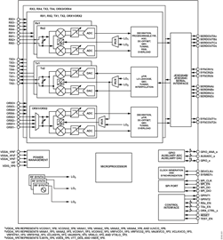
The ADRV9026 is a highly integrated, radio frequency (RF) agile transceiver offering four independently controlled transmitters, dedicated observation receiver inputs for monitoring each transmitter channel, four independently controlled receivers, integrated synthesizers, and digital signal processing functions providing a complete transceiver solution. The device provides the performance demanded by cellular infrastructure applications, such as small cell base station radios, macro 3G/4G/5G systems, and massive multiple in/multiple out (MIMO) base stations.
The receiver subsystem consists of four independent, wide bandwidth, direct conversion receivers with wide dynamic range. The four independent transmitters use a direct conversion modulator resulting in low noise operation with low power consumption. The device also includes two wide bandwidth, time shared, observation path receivers with two inputs each for monitoring transmitter outputs.
The complete transceiver subsystem includes automatic and manual attenuation control, dc offset correction, quadrature error correction (QEC), and digital filtering, eliminating the need for these functions in the digital baseband. Other auxiliary functions such as analog-to-digital converters (ADCs), digital-to-analog converters (DACs), and general-purpose input/outputs (GPIOs) that provide an array of digital control options are also integrated.
To achieve a high level of RF performance, the transceiver includes five fully integrated phase-locked loops (PLLs). Two PLLs provide low noise and low power fractional-N RF synthesis for the transmitter and receiver signal paths. A third fully integrated PLL supports an independent local oscillator (LO) mode for the observation receiver. The fourth PLL generates the clocks needed for the converters and digital circuits, and a fifth PLL provides the clock for the serial data interface.
A multichip synchronization mechanism synchronizes the phase of all LOs and baseband clocks between multiple ADRV9026 chips. All voltage controlled oscillators (VCOs) and loop filter components are integrated and adjustable through the digital control interface.
The serial data interface consists of four serializer lanes and four deserializer lanes. The interface supports both the JESD204B and JESD204C standards, operating at data rates up to 12.288 Gbps. The interface also supports interleaved mode for lower bandwidths, thus reducing the number of high speed data interface lanes to one. Both fixed and floating-point data formats are supported. The floating-point format allows internal automatic gain control (AGC) to be invisible to the demodulator device.
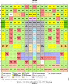
The ADRV9026 is powered directly from 1.0 V, 1.3 V, and 1.8 V regulators and is controlled via a standard serial peripheral interface (SPI) serial port. Comprehensive power-down modes are included to minimize power consumption in normal use. The ADRV9026 is packaged in a 14 mm × 14 mm, 289-ball chip scale ball grid array (CSP_BGA).
Applications
- 3G/4G/5G TDD and FDD massive MIMO, macro and small cell base stations
This product has been released to the market. The data sheet contains all final specifications and operating conditions. For new designs, ADI recommends utilization of these products.


