
- Manufacturer Part Number : LTC5530
- Manufacturer : AD
- Description : Precision 300MHz to 7GHz RF Detector with Shutdown and Gain Adjustment
- Series : LTC5530
- Reference Price : USD 0
- Our Price : We have a better price, contact us by email
- Product Type : RF Power Detectors
- Function : Envelope Detectors & Peak Detectors
- Current Suggest : Production
- Status : Production
- RoHS Status: -
- Voltage: -
- Feature: -
- Package Case: -
- Temperature Range: -
- Packing: Reel/Tray/Tube
- Standard Packing Quantity: -
- Country of Origin: -
- Other Part Number : LTC5530
- Shipping methods : DHL FEDEX UPS TNT
- Delivery Time : Ship within 1 day.
- Manufacturer Production time : 6-8 weeks (Normally have stocks)
- Weight : 0.001KG
Contact us to check the best price and real time inventory quantity for LTC5530. If you need any more information about LTC5530, you can also send us by email. Our email is [email protected], we will reply you in 12 hours.
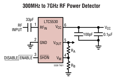
The LTC5530 is an RF power detector for RF applications operating in the 300MHz to 7GHz range. A temperature compensated Schottky diode peak detector and buffer amplifier are combined in a small ThinSOT™ package. The supply voltage range is optimized for operation from a single lithium-ion cell or 3xNiMH.
The RF input voltage is peak detected using an on-chip Schottky diode. The detected voltage is buffered and supplied to the VOUT pin. The output buffer gain is set via external resistors. A power saving shutdown mode reduces current to less than 2µA.
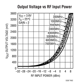
The LTC5530 operates with input power levels from -32dBm to 10dBm.
*Higher frequency operation is achievable with reduced performance. Consult factory for more information.
Applications
- 802.11a, 802.11b, 802.11g, 802.15, 802.16
- Multimode Mobile Phone Products
- Optical Data Links
- Wireless Data Modems
- Wireless and Cable Infrastructure
- RF Power Alarm
- Envelope Detector
At least one model within this product family is in production and available for purchase. The product is appropriate for new designs but newer alternatives may exist.


